The Complete Guide to Chemical Etching for Metching Hardware Manufacturing
- zhang qun
- Apr 11
- 20 min read

Table of Contents
· Key Takeaways
· What Is Chemical Etching for Hardware (What)
o Defining Chemical Etching
o Chemical Etching vs. Stamping vs. Laser Cutting
o Critical Numbers Every Buyer Should Know
· Who Uses Chemically Etched Hardware (Who)
o OEM Manufacturers and Brand Owners
o Product Engineers and R&D Teams
o Trading Companies and Global Sourcing Teams
· Where Chemically Etched Parts Are Used (Where)
o Consumer Electronics and Semiconductors
o Automotive and New Energy Vehicles
o Home Appliances and Kitchen Hardware
o Medical Devices and Precision Instruments
o Decorative Hardware and Signage
· Why Choose Chemical Etching Over Other Processes (Why)
o Precision and Batch Consistency
o Zero Tooling Investment
o Stress-Free Material Integrity
o Speed and Flexibility
· How Chemical Etching Works: A Step-by-Step Breakdown (How)
o Step 1: Metal Sheet Preparation
o Step 2: Photoresist Lamination and UV Exposure
o Step 3: Developing the Image
o Step 4: Chemical Etching
o Step 5: Stripping, Cleaning, and Post-Processing
o Step 6: Inspection and Packaging
· Six Buyer Pain Points and How to Solve Them
o Pain Point 1: Wildly Different Quotes for the Same Part
o Pain Point 2: Samples Pass, Mass Production Fails
o Pain Point 3: Suppliers Promise Tolerances They Cannot Hold
o Pain Point 4: Surface Finish Doesn't Match Expectations
o Pain Point 5: Delivery Dates Keep Slipping
o Pain Point 6: Missing Compliance Documents
· Cost Structure of Chemically Etched Hardware
· How to Choose a Reliable Chemical Etching Supplier
· Frequently Asked Questions
Key Takeaways
Chemical etching is a subtractive manufacturing process that uses acidic or alkaline solutions to selectively dissolve metal, producing precision hardware components with tolerances as tight as ±0.025 mm on sheet thicknesses ranging from 0.005 mm to 2.0 mm. Because the process requires no hard tooling, first samples can be delivered in as few as 1–3 working days, making it exceptionally well suited for complex patterns, thin-wall structures, and low-to-mid volume production runs. For procurement professionals and engineers, understanding how this process actually works—its capabilities, its limits, and where the costs really sit—translates directly into better sourcing decisions and fewer surprises on the production floor.
What Is Chemical Etching for Hardware (What)
Defining Chemical Etching
Chemical etching—also referred to as photochemical machining (PCM), chemical milling, or photo etching—is a metal removal process that uses chemical solutions to dissolve unprotected areas of a metal sheet, leaving behind the desired part geometry. The basic principle is straightforward: coat the metal with a light-sensitive resist, expose a pattern using UV light, develop away the unexposed resist, and then spray the sheet with an etchant that dissolves the bare metal. No cutting tools touch the workpiece. No dies slam into it. No laser beams heat it up. The metal's original mechanical properties come through the process completely intact.
That simplicity, however, masks a demanding manufacturing reality. At the industrial level, a competent etching facility must tightly control dozens of interacting parameters. The ferric chloride etchant concentration typically needs to stay within 36°Bé–42°Bé (Baumé scale). Solution temperature runs between 45°C and 55°C. Spray nozzle pressure sits in the 1.5–3.0 kg/cm² range. Conveyor speed, dissolved metal ion content, resist thickness, UV exposure duration—all of these variables interact, and a drift in any single one shows up immediately in dimensional accuracy and surface quality. Getting a clean etch on 50 prototype pieces is one thing. Holding that quality across 500,000 pieces over three months of continuous production is an entirely different challenge.
Chemical Etching vs. Stamping vs. Laser Cutting
Buyers evaluating chemical etching almost always ask the same question first: "Why wouldn't I just stamp this, or laser-cut it?" The honest answer is that it depends on your part geometry, your material, and your volume.
Stamping is king when it comes to raw speed. A high-speed progressive die press can punch out hundreds of parts per minute, driving per-piece costs down to fractions of a cent at high volumes. But stamping has a hard prerequisite: you need a die. A precision progressive die costs anywhere from $5,000 to $80,000, takes 3–8 weeks to manufacture, and commits you to one specific design. If your part has complex perforations—say a filter screen with thousands of micro-holes—the die becomes exponentially more difficult and expensive to build and maintain. On materials thinner than 0.1 mm or harder than HRC 40, stamping introduces burrs, micro-cracks, and deformation that may not be acceptable.
Laser cutting eliminates the tooling problem entirely. You go straight from a CAD file to cut parts. But laser cutting is a sequential process—the beam traces each contour one at a time. A mesh screen with 5,000 holes means the laser has to cut 5,000 individual holes. Chemical etching dissolves all 5,000 simultaneously, regardless of quantity. Laser cutting also creates a heat-affected zone (HAZ) along every cut edge, typically 0.05–0.2 mm wide, where the material's microstructure has been altered. On thin foils below 0.2 mm, this HAZ can cause warping, discoloration, and localized brittleness.
Chemical etching's core competitive advantage is this: it processes all features simultaneously, requires no hard tooling, and introduces zero mechanical or thermal stress into the material. Its limitations are equally clear: it struggles with thick materials (the practical economic ceiling is about 1.5 mm, with 2.0 mm as the hard limit for most metals), tolerances widen proportionally with thickness, and the process involves chemical handling and waste treatment that demand environmental compliance infrastructure.
Critical Numbers Every Buyer Should Know
These figures form the foundation of any process selection or supplier evaluation:
Workable thickness range: 0.01 mm–2.0 mm. The sweet spot for cost-efficiency is 0.05 mm–1.0 mm.
Standard tolerance: ±10% of material thickness, with a floor of ±0.025 mm. For a 0.5 mm stainless steel sheet, that means ±0.05 mm.
Minimum feature size (line width or slot width): approximately 80%–100% of material thickness. A 0.2 mm thick copper sheet can reliably hold features down to 0.16–0.2 mm.
Surface roughness: Ra 0.4 μm–1.6 μm, depending on material and etch parameters.
Prototype lead time: 3–7 working days including phototool production.
Production lead time: typically 7–15 working days, depending on volume and post-processing requirements.
Phototool cost: typically $70–$300 USD, a fraction of a stamping die investment.
Who Uses Chemically Etched Hardware (Who)
OEM Manufacturers and Brand Owners
The largest buyers of chemically etched hardware are OEM manufacturers in consumer electronics, automotive components, medical devices, and home appliances. These companies have defined drawings, material specifications, and quality standards, and they need suppliers who can deliver to print consistently.
Consider consumer electronics. A single smartphone may contain 3–8 chemically etched metal components: EMI shielding cans, contact springs, thermal copper foils, SIM tray liners, and speaker mesh screens. A handset brand shipping 30 million units per year needs 90–240 million etched parts annually just for these applications. At this scale, chemical etching's ability to nest hundreds of parts on a single large panel and process them in one pass makes it fully competitive with stamping on throughput.
The automotive sector drives equally significant volumes. In a battery electric vehicle, the battery management system (BMS) alone uses etched nickel busbars, electrode spacers, and sensor springs. A single battery module may require 50–200 etched nickel or copper pieces. Multiply that by the number of modules per vehicle and the annual production volume of a major EV maker, and you reach quantities in the hundreds of millions per year.
Product Engineers and R&D Teams
For engineers in the product development phase, chemical etching's biggest draw is design freedom during iteration. When you need to test three different spring geometries or evaluate two hole-pattern variants on a filter screen, chemical etching lets you do it fast and cheap. Change the CAD file, produce a new phototool for a couple hundred dollars, and have new samples in hand within a week. Modifying a stamping die for the same design change would cost thousands of dollars and weeks of lead time.
A structural engineer at a consumer electronics company once put it to me this way: "Chemical etching lets me get the function right first without worrying about die constraints. I can always switch to stamping later for mass production if the economics justify it." That "validate first, invest later" philosophy is critical in industries where product lifecycles are measured in months, not years.
Trading Companies and Global Sourcing Teams
If you run a hardware trading business or source metal components for overseas clients, chemical etching's low minimum order quantities are a major advantage. Stamping typically requires MOQs of 5,000–10,000 pieces or more to amortize die costs. Chemical etching MOQs can drop to 100 pieces or even fewer.
This means you can test market response with minimal commitment. Want to pitch a custom stainless steel bookmark, a branded metal business card, or a decorative badge to a new client? Order 50–100 sample pieces for under $300 total, ship them out for evaluation, and only commit to a larger run once the order is confirmed. The financial risk profile is fundamentally different from tooling-dependent processes.
Where Chemically Etched Parts Are Used (Where)
Consumer Electronics and Semiconductors
This is one of the highest-volume downstream applications for chemical etching.
EMI shielding cans sit on top of PCB assemblies to block electromagnetic interference between chips. They are typically made from nickel silver (C7521) or stainless steel (SUS304), 0.1–0.3 mm thick, with nickel or tin plating. A 5G smartphone may require 5–12 shielding cans of varying sizes, each with precise dimensional requirements to fit tightly onto the PCB.
Contact springs and connector clips provide electrical connection in battery compartments, SIM card slots, and button assemblies. These parts demand excellent elasticity and conductivity, so they are usually etched from phosphor bronze (C5191) or beryllium copper (C1720) in thicknesses of 0.05–0.15 mm.
Lead frames are the structural backbone of semiconductor packages, connecting the die to external circuitry. Chemically etched lead frames can achieve line widths down to 0.1 mm, supporting high-density packaging formats like QFN and BGA.
Thermal copper foils with thicknesses of 0.03–0.1 mm are etched into specific heat-conduction pathways and bonded to chip surfaces for thermal management in high-performance processors and power modules.
Automotive and New Energy Vehicles
The rapid growth of electric vehicles has created a wave of new demand for chemical etching. Inside a battery pack, etched nickel busbars connect individual cell terminals. Etched copper tabs serve as electrode connectors. Temperature sensor springs and insulation spacers—components that need tight tolerances, burr-free edges, and zero residual stress—are tailor-made for this process.
In a typical prismatic cell module, each cell requires 2–4 etched nickel or copper connectors. One module contains dozens of cells, and a single vehicle carries multiple modules. Working the math on a manufacturer producing 500,000 vehicles per year, the annual consumption of etched connectors alone reaches 100–250 million pieces.
Beyond battery systems, automotive pressure sensors, mass airflow sensors, and fuel cell bipolar plates all rely on chemically etched metal components. Sensor diaphragms, for instance, require thickness uniformity within ±5 μm and absolutely burr-free edges—requirements that chemical etching meets naturally.
Home Appliances and Kitchen Hardware
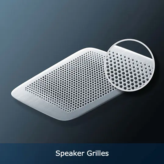
Coffee machine filter screens, tea infusers, showerhead faceplates, dishwasher filter discs, air purifier mesh panels—these everyday household hardware items are produced by the millions through chemical etching.
Take a coffee machine filter screen. A typical disc, perhaps 60 mm in diameter, may feature 10,000+ micro-holes ranging from 0.1 mm to 0.3 mm in diameter, with hole-to-hole spacing controlled to 0.05 mm. Stamping cannot produce holes this fine (the punch pins would snap). Laser cutting can do it, but must cut each hole sequentially, making production prohibitively slow. Chemical etching forms every hole simultaneously, delivers burr-free edges suitable for food contact, and maintains hole-diameter consistency within ±0.03 mm.
Showerhead faceplates follow similar logic. High-end showerheads require uniform water distribution, which depends on consistent hole sizes across several hundred openings. Double-sided chemical etching controls each hole's diameter to within ±0.03 mm, ensuring even flow.
Medical Devices and Precision Instruments
The medical industry imposes some of the most demanding requirements on metal components: zero burrs (to prevent tissue damage), zero residual stress (to guarantee long-term dimensional stability), and full material traceability (to comply with FDA 21 CFR Part 820 and EU MDR). Chemical etching inherently satisfies the first two, and mature suppliers provide complete material certificates and process records for the third.
Specific applications include microneedle arrays for transdermal drug delivery, blood filtration screens, precision graduated scales on surgical instruments, textured surfaces on orthopedic implants to promote bone integration, and microfluidic channel layers in gene sequencing chips.
Decorative Hardware and Signage
Chemical etching has the longest history in the decorative space. Metal logos for luxury brands, hotel room number plates, metal nameplates on premium packaging, commemorative coins, and metal bookmarks continue to be produced using this process in large volumes.
These products are characterized by intricate artwork, flexible batch sizes (from a few dozen to tens of thousands), and demanding post-processing sequences (color filling, electroplating, brushing, PVD coating, and more). Chemical etching's irreplaceable advantage here is its ability to create genuine three-dimensional relief on a metal surface—recessed areas versus raised areas—with a tactile quality that printing and laser marking simply cannot replicate.
Why Choose Chemical Etching Over Other Processes (Why)
Precision and Batch Consistency
Chemical etching delivers tolerances at the ±0.025 mm level, which is adequate for the vast majority of precision hardware applications. But the more important story is not single-piece accuracy—it is batch-to-batch consistency.
A stamping die's accuracy degrades as the tool wears. After 500,000 strokes, the punch-die clearance that started at 0.01 mm may have opened up to 0.03–0.05 mm. You compensate by regrinding or replacing the die, which costs money and time. Chemical etching has no wear mechanism because no physical tool contacts the workpiece. The dimensional consistency between the first piece and the 100,000th piece depends on solution chemistry, not mechanical wear. As long as the etchant parameters are monitored and maintained—and any serious supplier has automated systems to do exactly that—the process naturally produces stable results across long production runs.
Zero Tooling Investment
This is the single most compelling argument for buyers in the product development phase.
Consider a straightforward comparison. You need a 30 mm × 20 mm part with a perforated pattern, etched from 0.3 mm SUS304 stainless steel.
The stamping route: die cost $5,000–$12,000, die lead time 4–6 weeks, per-piece cost at 100,000 units approximately $0.01–$0.04.
The chemical etching route: phototool cost $70–$200, sample lead time 3–5 working days, per-piece cost at 100,000 units approximately $0.04–$0.10.
If your initial order is 100,000+ pieces and your design is frozen—stamping wins on total cost. But if you are still in validation, if your order is 1,000–10,000 pieces, or if there is any chance you will need to revise the design two or three times, chemical etching's total cost of ownership is dramatically lower. Each stamping die modification runs $1,000–$3,000 and takes 1–2 weeks. Each chemical etching design revision requires only a new phototool for under $200.
Stress-Free Material Integrity
This matters most for spring contacts and thin-wall components.
During stamping, the shearing force at the punch edge creates residual stress and micro-cracks in the cut zone. For spring components subjected to repeated deflection, these micro-cracks can propagate over thousands of cycles and eventually cause fatigue failure. Industry data suggests that stamped springs typically exhibit 20%–40% lower fatigue life compared to chemically etched springs of the same design, though exact figures depend on material and geometry.
Laser cutting introduces a heat-affected zone where the material has undergone rapid melting and resolidification. Within 0.05–0.2 mm of the cut edge, the grain structure differs from the base material, and both hardness and ductility are altered. For parts that will be welded downstream, this HAZ can cause inconsistent weld quality.
Chemical etching is a purely chemical dissolution process. No force, no heat. Parts come off the etching line with material properties identical to the original sheet stock.
Speed and Flexibility
From order placement to delivery, the standard chemical etching timeline looks like this:
Phototool production: 1–2 working days. First article confirmation: 1–2 working days. Mass production (using a 10,000-piece run as a reference): 3–5 working days. Post-processing such as plating or forming, if required: 2–5 working days.
Total: roughly 7–14 working days. Compare that to stamping, where the path from die design through manufacturing, trial runs, and first production typically takes 6–10 weeks.
This speed advantage proves critical in two common scenarios. The first is product launches with fixed deadlines—a consumer electronics brand that needs all components ready before a global launch event cannot afford an 8-week die cycle. The second is emergency replenishment—when a production line runs short on a specific component and needs a few thousand pieces within a week to avoid shutting down.
How Chemical Etching Works: A Step-by-Step Breakdown (How)
Step 1: Metal Sheet Preparation
Everything starts with a clean sheet of metal. When raw material arrives at the factory, incoming inspection verifies the alloy grade, thickness, temper condition, and surface quality against the order specification. A common example: SUS304 stainless steel, 0.3 mm ±0.02 mm, half-hard temper (1/2H), bright annealed (BA) surface finish.
Sheets that pass inspection enter the cleaning line. Industrial-grade cleaning typically follows a three-stage alkaline degrease → acid activation → deionized water rinse sequence. The alkaline wash removes oils and fingerprints (which is why operators must never touch the sheet with bare hands—a fingerprint is only about 0.1 μm thick, but that thin film of skin oil is enough to compromise photoresist adhesion). The acid dip removes light surface oxides. The DI water rinse eliminates chemical residue. Cleaned sheets are dried in 60°C–80°C forced hot air, then move directly to lamination.
Step 2: Photoresist Lamination and UV Exposure
Dry film photoresist is applied to both sides of the cleaned metal sheet using heated lamination rollers. Lamination temperature is typically controlled between 100°C and 120°C, with roller pressure at 0.3–0.5 MPa. The goal is full adhesion with zero air bubbles or wrinkles between the resist film and the metal surface.
The laminated sheet then moves into the exposure unit. The phototool—a film negative carrying the part pattern—is placed in tight contact with the resist surface, and ultraviolet light (wavelength 350–420 nm) is projected through it. Exposure time typically falls between 8 and 15 seconds, depending on the resist type and thickness.
Where UV light hits the resist, a crosslinking reaction occurs: the polymer chains bond together, making the resist hard and insoluble in the developer. Where the phototool's opaque pattern blocks the light, the resist remains soft and soluble.
Step 3: Developing the Image
The exposed sheet enters the developing line, where a 1%–1.5% sodium carbonate (Na₂CO₃) solution washes across both surfaces. The uncrosslinked resist dissolves and washes away, exposing the bare metal underneath. The crosslinked resist remains firmly bonded to the metal, forming a protective mask.
After this step, the sheet presents a clear pattern: areas covered by hardened resist define the parts you want to keep; bare metal areas will be dissolved in the next step.
The critical quality metric here is the "development factor"—essentially the verticality of the resist wall at the pattern edge. Ideally, the resist cross-section should be nearly perpendicular to the metal surface, so that the etch boundary is sharp and well-defined. Under-development (resist residue remaining on bare areas) leads to incomplete etching. Over-development (resist edges eroded inward) causes undersized features.
Step 4: Chemical Etching
This is the core of the entire process. The developed sheet enters the etching machine, where heated etchant is sprayed uniformly onto both sides through upper and lower nozzle arrays.
For stainless steel and copper alloys, the most widely used etchant is ferric chloride (FeCl₃) solution, maintained at 36°Bé–42°Bé concentration and 45°C–55°C temperature. Etch rate varies with material, temperature, and dissolved metal ion loading. As a general guide:
0.1 mm copper: approximately 1–2 minutes.0.3 mm SUS304 stainless steel: approximately 4–8 minutes.0.5 mm SUS304 stainless steel: approximately 8–15 minutes.
An unavoidable physical phenomenon called undercut occurs during etching. The etchant doesn't only dissolve metal downward—it also attacks laterally, creeping under the resist edges. The undercut distance is typically 10%–25% of the material thickness. An experienced factory compensates for this at the phototool design stage, adjusting feature dimensions so that the final etched part lands on target.
This is also why thicker material means wider tolerances. On 0.1 mm material, the undercut is roughly 0.01–0.025 mm. On 1.0 mm material, it may reach 0.1–0.25 mm. This relationship directly defines the economic thickness ceiling for chemical etching.
Step 5: Stripping, Cleaning, and Post-Processing
After etching, the remaining photoresist is stripped from the metal using a 3%–5% sodium hydroxide (NaOH) solution. The sheet then passes through multiple DI water rinse stages and hot-air drying to yield clean, bare metal parts.
Depending on the application, subsequent operations may include:
Electroplating—nickel, gold, tin, silver, or zinc plating to improve corrosion resistance, electrical conductivity, solderability, or appearance. EMI shielding cans, for instance, commonly receive a nickel undercoat (1.0–3.0 μm) followed by a tin topcoat (3.0–8.0 μm).
Surface finishing—brushing, bead blasting, polishing, PVD coating, or anodizing (for aluminum parts).
Forming—many parts require bending after etching. Shielding cans, for example, need their sidewalls folded up to create a box shape.
Film lamination or assembly—some parts ship with protective films applied, or are assembled with other components before packaging.
Step 6: Inspection and Packaging
Standard quality checks for chemically etched hardware include visual inspection under 10×–30× magnification for surface defects, dimensional measurement on a vision measuring system (typical instrument accuracy ±0.001 mm), thickness verification with a micrometer or coating thickness gauge, and functional testing where applicable (spring force values for contact springs, flow-rate testing for filter screens, and so on).
Packaging varies by part type. Precision springs are typically placed individually into anti-static trays. Decorative pieces are separated by foam inserts to prevent scratches. High-volume standard parts may ship in poly bags inside corrugated cartons.
Six Buyer Pain Points and How to Solve Them
Pain Point 1: Wildly Different Quotes for the Same Part
You send the same drawing to three suppliers. The quotes come back varying by 50% or more. This doesn't necessarily mean someone is overcharging you—more often, it means each supplier interpreted the requirements differently.
The fix: when issuing an RFQ, always specify the complete picture beyond just the drawing. State the exact alloy grade and temper (e.g., "SUS304 2B" versus "SUS304 BA"—they are priced differently). Define the tolerance tier (standard versus tight tolerance changes the process difficulty significantly). Spell out surface treatment requirements including plating type, plating thickness, and any appearance criteria. Provide an annual volume forecast so the supplier can amortize fixed costs realistically. State the inspection standard—whether you require PPAP, FAI reports, or need parts to meet industry-specific certifications. The more complete your RFQ package, the more accurate and comparable the quotes will be.
Pain Point 2: Samples Pass, Mass Production Fails
This is a classic problem. Samples come through perfectly—dimensions on target, surfaces clean, everything looks right. Then you place a 100,000-piece production order and discover an 85% yield rate, with 15% of parts showing over-etching, dimensional drift, or surface staining.
The root cause almost always traces back to one of three issues. First, during sampling the supplier used fresh etchant at optimized parameters—essentially hand-crafting each piece. In mass production, etchant condition fluctuates and the same level of individual attention is impossible. Second, operators who carefully monitored a 50-piece sample run cannot maintain that same vigilance across weeks of volume production under capacity pressure. Third, the raw material lot used for samples may differ slightly in thickness, hardness, or surface condition from the production lot.
The fix: when approving samples, request the process parameter records (etchant concentration, temperature, etch time) used during the sample run. Before mass production, confirm that the supplier uses an SPC (Statistical Process Control) system to monitor critical parameters in real time. Agree on a clear incoming quality standard and a formal procedure for handling non-conforming parts. If your order is high-value or high-risk, conduct an on-site process audit during the first production batch.
Pain Point 3: Suppliers Promise Tolerances They Cannot Hold
Some suppliers agree to any tolerance requirement to win the order, but their actual process capability falls short. A buyer requests ±0.02 mm (achievable on 0.1 mm thin material), but the supplier's equipment and process control can only reliably deliver ±0.05 mm. The gap only becomes visible after parts are delivered and measured.
The fix: let data do the talking. During the sample phase, require the supplier to submit a first article inspection report with actual measured values—not handwritten approximations, but instrument-generated data. Insist on measuring at least 30 pieces for each critical dimension and calculate the Cpk value. A Cpk ≥ 1.33 indicates the supplier's process can stably meet your tolerance. A Cpk between 1.0 and 1.33 warrants caution. Below 1.0, the supplier almost certainly cannot hold your requirement consistently.
Pain Point 4: Surface Finish Doesn't Match Expectations
Post-etch parts sometimes look different from what you envisioned. Common complaints include uneven brightness on etched stainless steel surfaces, color variation between plating batches (one lot of nickel-plated parts looks darker than the previous one), and color-fill ink peeling off decorative parts after a period of use.
The fix: for any part with meaningful appearance requirements, establish a signed-off master sample (a physical reference piece that both parties agree represents the acceptable standard). Understand the process steps that drive appearance: surface roughness after etching determines how plating or paint will adhere and reflect light; the quality of pre-plating activation and strike layers determines plating uniformity; the ink type and curing method used for color fill determines adhesion durability. Require the supplier to create SOPs for each appearance-critical operation and to check each production batch against the master sample.
Pain Point 5: Delivery Dates Keep Slipping
The supplier promises 15-day delivery. On day 12 you hear that production hasn't started—raw material arrived late, the production schedule is backed up, a previous order ran over.
The fix: at order placement, agree on a production schedule with defined milestones—when will the phototool be ready, when does exposure begin, when does the lot enter the etch line, when does post-processing finish, when can shipment occur. Require proactive status updates at each milestone. If your delivery timeline is business-critical, consider contractual late-delivery penalties. Maintain a pool of 2–3 qualified suppliers to avoid single-source risk.
Pain Point 6: Missing Compliance Documents
If your products ship to the EU, North America, or Japan, you may need your supplier to provide RoHS test reports, REACH compliance declarations, Conflict Minerals (CMRT) documentation, or even California Proposition 65 compliance evidence. Many small and mid-sized etching factories are weak in this area—they either cannot provide the documents at all or produce paperwork that your compliance team rejects.
The fix: make compliance documentation a hard gate at the supplier qualification stage. Request RoHS test reports from accredited third-party labs (SGS, TÜV, Intertek, Bureau Veritas). Obtain MSDS and REACH registration data for plating chemicals. Verify that the factory holds an ISO 14001 environmental management certification. For products destined for Europe, confirm that the supplier tracks and can declare against the latest version of the REACH SVHC (Substances of Very High Concern) candidate list.
Cost Structure of Chemically Etched Hardware
Understanding where the money goes helps you negotiate smarter and spot unreasonable pricing.
The cost of a chemically etched part typically breaks down as follows:
Raw material accounts for 30%–55% of total cost, depending heavily on alloy type—copper alloys and titanium are far more expensive per kilogram than standard stainless steel. Material utilization rate is a critical lever: a well-optimized nesting layout can push utilization from 60% up to 85% or higher, directly reducing the per-piece material charge.
Phototool and setup costs are one-time charges, typically $70–$300 USD. Amortized across a large order, they become negligible. On a small order of 200 pieces, however, they add meaningful per-piece cost.
Processing costs (the full sequence of cleaning, lamination, exposure, developing, etching, and stripping) typically represent 25%–40% of total cost. Interestingly, processing cost is largely independent of pattern complexity—the etchant does not charge extra for intricate designs. The primary driver is material thickness, because thicker sheets require longer etch times and consume more line capacity.
Post-processing costs (plating, forming, lamination, etc.) are the most variable component, ranging from zero for parts that ship as-etched to 30%–50% of total cost for parts requiring gold plating, bending, protective film application, and individual packaging.
Inspection and packaging typically account for 3%–8% of total cost. Special inspection requirements such as 100% inspection, salt spray testing, or X-ray analysis can push this figure higher.
How to Choose a Reliable Chemical Etching Supplier
Price comparison alone is not a supplier selection strategy. Here are the dimensions I recommend buyers evaluate:
Equipment capability matters more than factory floor area. Look at the etching line's maximum panel size, the minimum and maximum thickness it can handle, and whether the line has automated etchant monitoring (in-line pH meters, Baumé sensors, and automatic temperature control). A production line with closed-loop chemical management produces fundamentally more stable output than one relying on operators to manually sample and adjust.
Quality management systems provide the framework for consistency. ISO 9001 is the baseline. Automotive buyers should require IATF 16949. Medical device buyers should look for ISO 13485 or, at minimum, demonstrated experience manufacturing medical components in a controlled cleanroom environment.
Industry-specific experience is not interchangeable. A factory with 15 years of EMI shielding production for smartphone OEMs and a factory that primarily makes decorative nameplates both perform chemical etching, but their process know-how, quality benchmarks, and capacity configurations can be completely different. Prioritize suppliers with proven track records in your specific application.
Capacity and scalability should be quantified. Understand the supplier's peak monthly capacity measured in square meters of processed sheet. Confirm their ability to ramp during your peak season. If your demand fluctuates significantly between quarters, verify that the supplier can absorb surges without sacrificing lead times.
Communication responsiveness is often underestimated but directly impacts total cost of ownership. A supplier that returns technical answers within 24 hours and provides DFM (Design for Manufacturability) feedback within 48 hours will save you more in avoided delays and design iterations than a supplier whose price is 5% lower but takes three days to respond to emails.
Frequently Asked Questions
What metals can be chemically etched?
Most industrial metals can be processed, including stainless steel (SUS301, SUS304, SUS316L, SUS430, and other grades), copper and copper alloys (pure copper C1100, phosphor bronze C5191/C5210, brass C2680, nickel silver C7521/C7701, beryllium copper C1720), nickel and nickel alloys (pure nickel N6, Inconel 625/718), aluminum and aluminum alloys (AL1050, AL5052, AL6061), titanium and titanium alloys (Grade 1/Grade 5), as well as molybdenum, tungsten, and various specialty alloys. Each metal requires specific etchant chemistry and process parameters.
What is the minimum order quantity?
Because no hard tooling is required, MOQs are highly flexible. Prototyping quantities can start as low as a handful of pieces. Small production orders start at 100 pieces with most suppliers. Be aware, however, that very small quantities (10–50 pieces) carry a higher per-piece cost because phototool and setup charges cannot be spread across enough units.
How precise can chemical etching be?
Standard tolerance is ±10% of material thickness, with a minimum of ±0.025 mm. On 0.1 mm material, expect ±0.025 mm. On 0.5 mm material, expect ±0.05 mm. Under tightened process controls, some suppliers can achieve narrower tolerances, but this increases cost and may reduce yield. The minimum achievable feature size (line width or aperture diameter) is approximately 80%–110% of material thickness.
What are the environmental impacts, and how is waste handled?
The ferric chloride etchant and the alkaline developing/stripping solutions used in chemical etching are classified as industrial waste and must be treated before discharge. Compliant factories operate wastewater treatment systems that precipitate heavy metal ions and neutralize pH to meet discharge standards. Metal content in spent etchant—particularly copper and iron ions—can be recovered and recycled. When selecting a supplier, verify that they hold valid environmental discharge permits and hazardous waste handling certifications.
What post-processing options are available for etched parts?
Virtually all standard metal finishing processes can be applied to chemically etched parts: electroplating (nickel, tin, gold, silver, zinc), electroless plating (electroless nickel, immersion gold), anodizing (aluminum only), passivation (stainless steel corrosion protection), PVD coating, painting, silk-screen printing, pad printing, brushing, bead blasting, polishing, heat treatment, and bending/forming. The choice depends on the part's functional and aesthetic requirements.
How long does it take from sending a drawing to receiving samples?
With the drawing confirmed and raw material in stock, the standard sample lead time is 1–3 working days for etching only. If electroplating or other post-processing is needed, total sample lead time extends to approximately 5–10 working days. Some factories offer expedited 1–3 day turnarounds for urgent projects, typically at a premium charge.

Comments