Silicon Photonics Alignment Masks: Control Datums Before Apertures
Updated: 1 day ago
A silicon photonics alignment mask rarely fails because the CAD aperture is the wrong shape. More often, the aperture field is correct in isolation but misplaced relative to the fixture datums, fiber array, package edge or optical reference. Once the plate enters a stacked test fixture, registration error accumulates across every interface.
SEMI's October 6, 2026 article Testing Silicon Photonics at Scale argues that photonic devices need test infrastructure capable of reliable, economic volume manufacturing. For a thin alignment plate, the practical priority is to control how the mask locates before tightening aperture dimensions.
A silicon photonics alignment mask is part of a stack
The mask may sit between a fixture frame and device carrier, define optical access, shield stray light or protect adjacent hardware during probing. Its position depends on pins, shoulders, pockets, fasteners and neighboring plates. If each component references a different origin, the final optical path can shift even when every part passes inspection.
Choose datums that physically exist in the assembled fixture. Two locating holes can establish translation and rotation; a controlled outside profile can locate in a pocket; a slot-and-hole pair can prevent overconstraint when temperature changes. State which features locate and which merely provide clearance.
Separate aperture size from aperture position
Aperture width controls available optical area, while position controls where that area lands. Combining both in one tight plus/minus dimension makes root-cause analysis difficult. Use basic location from functional datums, then apply an appropriate profile or position control to the field.
The allowable position error must come from the optical budget. Include fiber-array placement, package placement, fixture repeatability and stage error. The metal plate should not receive the entire system tolerance simply because it is easy to dimension.
Thin-sheet behavior changes inspection
A large open window can leave narrow rails that twist during handling. A dense aperture field distributes stiffness differently and increases fragile webs. Material grain, incoming flatness and pattern symmetry affect how the free plate behaves.
Define whether inspection occurs on a support plate, under light restraint or free state. A vision system can report excellent aperture position while vacuum-holding the plate flat, yet the part may lift during assembly. The support condition should reflect use.
Material and finish are optical decisions
Stainless steel offers practical stiffness and handling. Nickel alloys may suit thermal or environmental needs. Blackening can reduce reflections, but finish thickness, adhesion and particulate control need review. A cosmetic black surface is not automatically an optical black surface.
If coating follows etching, decide whether aperture size applies before or after coating. Buildup matters when an opening is narrow or two coated edges define a slit. Protect locating surfaces if coating would shift the plate.
Where photo etching fits the pattern
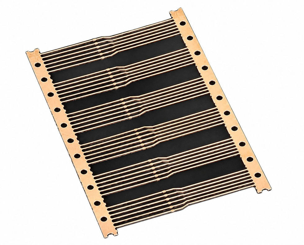
Photo etching is useful when one thin plate combines many apertures, fiducials, mounting features and complex outlines. The artwork can include half-etched identification or assembly marks. Digital tooling supports revisions during fixture development.
The process is not universal. An etched wall is not perfectly vertical, so narrow optical edges must be evaluated against thickness and illumination direction. Laser may be faster for a few larger openings, but heat-affected edge and recast conditions matter. Wire EDM or CNC is better for thicker rigid masks requiring vertical walls, pockets or three-dimensional reference surfaces.
Inspection needs a shared coordinate system
Report the aperture field relative to the same datums used by the fixture. Include fiducials recognized by both the component supplier and assembly station. For repeated arrays, control the global pattern first, then identify locally critical apertures separately.
Do not use a scanned PDF as the manufacturing master for dense coordinates. Supply DXF or another unambiguous two-dimensional file plus a dimensioned PDF defining datums, tolerances, finish and inspection notes.
Key takeaways: locate the plate from functional fixture datums; budget position across the optical stack; specify the support condition; define aperture size before or after finish; and control the digital revision.
Frequently Asked Questions
Can half-etched fiducials be added?
Often yes, provided their depth and location do not weaken a rail or interfere with optics. Treat them as manufacturing aids, not precision reference surfaces unless verified.
Does chemical etching create a vertical aperture wall?
No. Etching produces a controlled chemical profile. If wall angle affects the optical path, include thickness, illumination direction and acceptable edge geometry in the review.
When should a rigid machined mask be used?
Use machining when the mask must provide a three-dimensional datum, deep counterbore, threaded feature or near-vertical wall through substantial thickness.
Sources and engineering context
SEMI, Testing Silicon Photonics at Scale, published October 6, 2026; accessed October 9, 2026. It describes the need for scalable silicon photonics test infrastructure as AI and HPC increase data movement. The DFM guidance here applies that context to a separately purchased thin metal fixture component.
Make the mask measurable in the same frame as the optics
A silicon photonics alignment mask should be accepted in the coordinate system that matters to the fiber array and device. Resolve the datum chain before the aperture field becomes a supplier dispute.
Metching's custom metal shim and spacer capability is relevant when a silicon photonics alignment mask also controls stack height. Send the mask drawing, datum definition, aperture file, material, thickness, finish and inspection plan for review.

Comments